Maxing out AES-128-CTR on a single Zen5 core
July 2, 2026 · github.com/samlaf/rust-cuda-aes
AES is the most widely deployed symmetric cipher in the world, encrypting most TLS traffic. Its main challenger, ChaCha20-Poly1305, was designed to win on CPUs lacking dedicated AES hardware — but that hardware is now everywhere, and 2025 benchmarks show hardware-accelerated AES beating ChaCha on every modern CPU.
Since ~2019, vectorized (SIMD) versions of AES, known as VAES, have been available, which theoretically allows quadrupling AES-NI’s throughput. And in the last 2 years, this hardware has become widely available enough for engineers to start seriously optimizing widely deployed AES software. Eric Biggers from Google has been pushing the state of the art in the Linux kernel with his Nov 2025 and Jan 2026 patch sets. He explains how he is modernizing the Linux kernel crypto API in his Jun 2026 talk. Dan Pittman of Intel also gave a talk at the OpenSSL conference in 2025 about Understanding Vectorization Through a New AES-XTS Implementation, which describes his openssl XTS PR.
In this article we will take a look at the physical limits of AES encryption on a single modern core. We show a series of 5 successive optimizations bringing a naive 0.47 GiB/s implementation all the way to a near-optimal 49 GiB/s on a single AMD Zen 5 core. The code is available on github.
- Background
- Benchmark Results
- Methodology
- 1.
cpu/scalar— baseline - 2.
cpu/aesni— hardware AES, one block at a time - 3.
cpu/aesni-x8— eight blocks at a time (Little’s law) - 4.
cpu/aesni-x8-pshufb— never leave the SIMD domain - 5.
cpu/vaes256-x8-pshufb— two blocks per instruction - 6.
cpu/vaes512-x8-pshufb— four blocks per instruction - 7. OpenSSL comparison
- Conclusion
- Appendix: Microarchitecture
Background
The goal of this article is not to explain how AES works 1 or how to implement it in software, but rather to focus on the performance aspects assuming modern CPUs with hardware acceleration for AES. For simplicity, and also to keep the article didactic and informative, we focus on AES-128 in CTR mode of operation 2, and restrict ourselves to a single core.
For completeness, we give just enough background information to contextualize the rest of the article.
Crypto Theory
At a super high level, a cipher is an algorithm that encrypts a plaintext into a ciphertext using a hidden key. Shannon explains that every cipher must uphold 2 properties:
- Confusion: hides the key (via nonlinearity 3) in the ciphertext
- Diffusion: hides the plaintext (via linear spreading) in the ciphertext
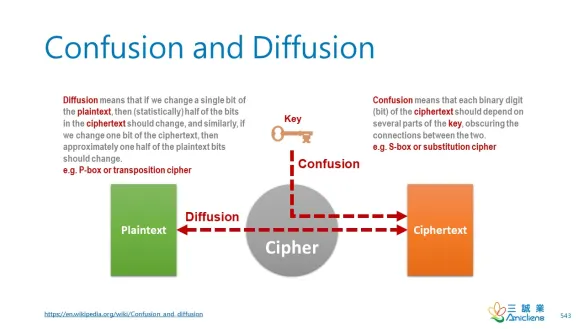
There are various classes of cipher designs. AES is a Substitution-Permutation Network (SPN), whose encryption process is depicted by this diagram4:
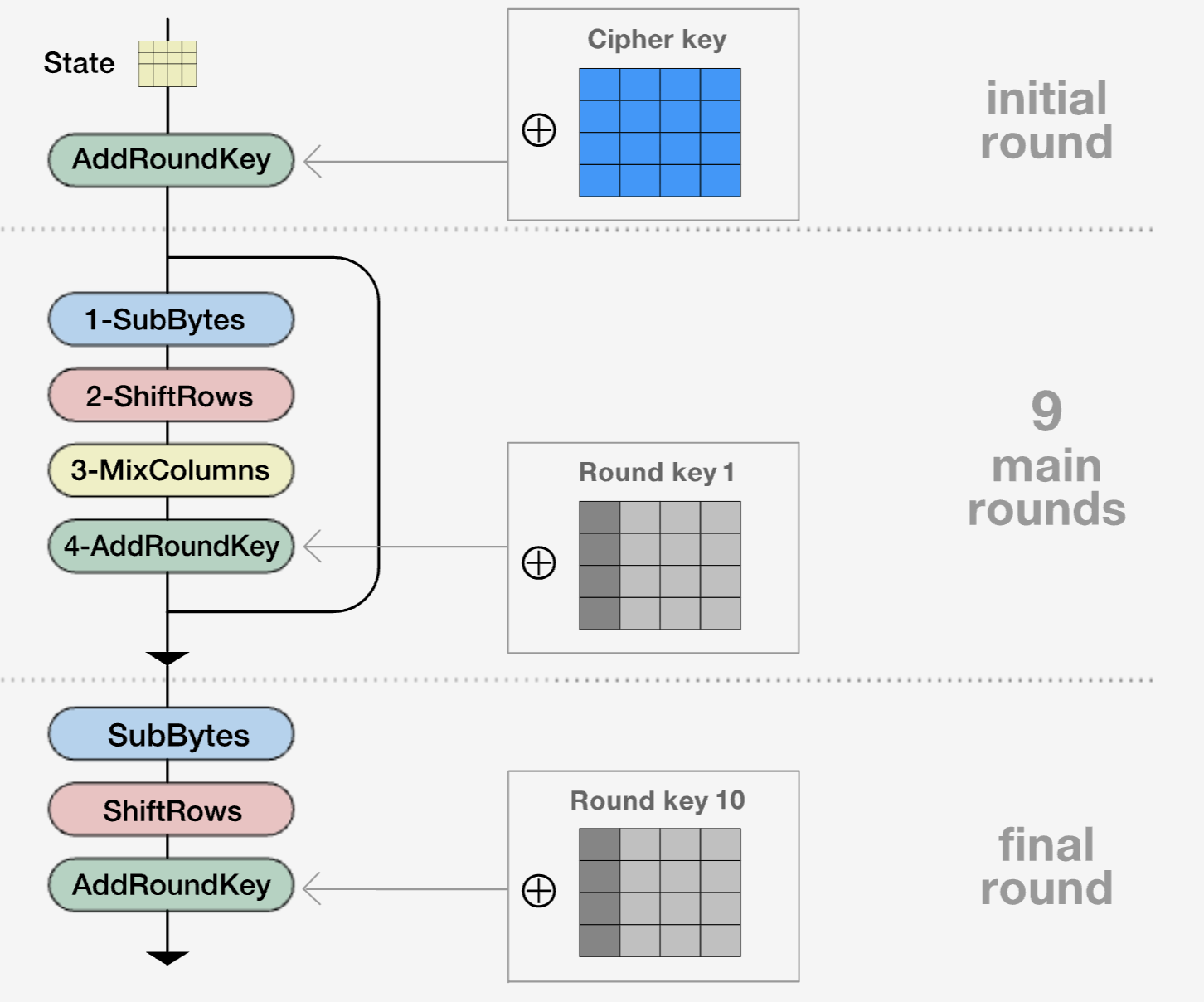
In SPNs, confusion is done via substitution (S-boxes), and diffusion is done via permutation. In AES specifically, confusion is done via AddRoundKey (which mixes the key into the state) followed by the SubBytes step, which is the S-box nonlinearity. Diffusion is done via the ShiftRows and MixColumns steps, both of which are linear.
Note that AES is a block cipher, meaning that the diagram depicted above only operates on fixed-size blocks of data (128 bits for AES). To encrypt payloads that are larger than 128 bits, AES blocks need to be chained somehow. The various ways to do so are called modes of operation.
Counter (CTR) mode which we focus on in this article turns the block cipher into a stream cipher 5:
ct[i] = pt[i] ⊕ E(k, counter₀ + i)
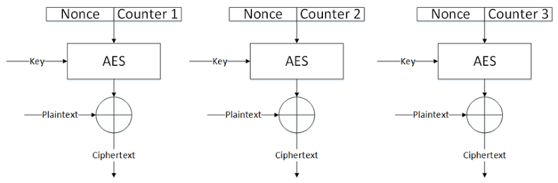
Importantly in this mode of operation, every 128-bit block of plaintext is encrypted independently, which means that multiple blocks can be processed in parallel.
Software implementations
There are four classic ways to implement AES in software — and all four are really S-box strategies, because the nonlinear SubBytes step is the only one whose cost can’t be precomputed away:
- Naive — compute every step directly: 16 S-box byte lookups, explicit ShiftRows, and a scalar MixColumns (~100 ops of shifts and XORs per round). Simple and slow.
- T-tables — widen the 16 S-box lookups to four 32-bit entries with the MixColumns coefficients pre-multiplied in, and instead of indexing and then shifting, use ShiftRows as the index pattern into the widened S-boxes. A full round collapses to 16 loads + 16 XORs.
- Daemen and Rijmen originally derived this optimization in their Rijndael AES-competition proposal, and it stayed the standard software implementation for a decade.
- However, T-tables are indexed by the plaintext and hence were shown to leak the key via cache-timing attacks (Bernstein, Osvik–Shamir–Tromer), so they are now considered insecure if not cache-hardened, which is why implementations have moved to the two approaches below, or to using AES-NI.
- Bitsliced — evaluate the S-box as a ~115-gate boolean circuit on bit-planes spread across SIMD registers, many blocks in lockstep (Käsper–Schwabe). The software throughput champion (~7 cyc/byte in 2009), but only for parallelizable modes (CTR/GCM) on long messages — it processes 8 blocks in lockstep and pays a transpose in and out of bit-plane form.
- Vector-permute — keep the S-box a table lookup, but move the table into a register:
PSHUFBdoes 16 parallel lookups into a 16-entry in-register table. The 256-entry S-box doesn’t fit a 4-bit index, so it’s reparameterized over a tower field GF((2⁴)²), which decomposes it into a handful of nibble-indexed 16-entry tables (Hamburg). Roughly T-table speed (~10–12 cyc/byte), works block-at-a-time, and constant-time since no lookup ever touches memory — this is OpenSSL’s vpaes fallback when AES-NI is absent.
Hardware acceleration
As we’ve seen above, AES software implementations need to be careful to avoid side channel attacks, and are slow, topping out at ~7 cycles/byte. Hardware circuitry was introduced to solve both of these problems 6: AES-NI in 2010, followed by ARMv8 AES in 2013, and finally VAES (256/512-bit) on Intel in 2019 and AMD in 2020/2022. This hardware completely blows any software implementation out of the water: the original non-vectorized AES-NI achieves a predicted throughput of ~0.31 cycles/byte on Zen5 7.
AES-NI itself is pretty simple and consists of four instructions 8: AESENC and AESDEC each doing one full AES round (SubBytes∘ShiftRows∘MixColumns then XOR round key), and AESENCLAST and AESDECLAST each doing the final AES round that lacks the MixColumns (SubBytes∘ShiftRows then XOR round key). These instructions work on a single 128-bit block in one XMM register. VAES is just those same opcodes re-encoded (VEX/EVEX) to operate on YMM (256-bit = 2 blocks) and ZMM (512-bit = 4 blocks). One vaesenc %zmm, %zmm, %zmm advances four independent counter blocks by one round, achieving 4x throughput.
Benchmark Results
We will walk through the six variants below:
| variant | throughput | cyc/byte | optimal ceiling | % of optimal ceiling |
|---|---|---|---|---|
cpu/scalar |
0.474 GiB/s | 8.90 | — | — |
cpu/aesni (x1) |
2.12 GiB/s | 1.96 | 0.31 | 16% |
cpu/aesni-x8 |
3.60 GiB/s | 1.15 | 0.31 | 27% |
cpu/aesni-x8-pshufb (128-bit) |
12.17 GiB/s | 0.341 | 0.31 | 92% |
cpu/vaes256-x8-pshufb (256-bit) |
23.96 GiB/s | 0.173 | 0.155 | 90% |
cpu/vaes512-x8-pshufb (512-bit) |
49.08 GiB/s | 0.0841 | 0.0775 | 93% |
We report throughput in GiB/s since it is a colloquial and human-friendly unit, and will be useful to compare with multicore variants that are memory bound. But for compute-bound work like this, seconds hide the clock and are an imprecise measure for the actual silicon performance which is subject to CPU throttling.
Furthermore, cycles/byte make it possible to compare against the microarchitecturally optimal performance, as reported in the last 2 columns. The AES-NI/VAES throughput ceiling is set by the AES execution units themselves, which on Zen5 have a reciprocal throughput of 0.5 7, and bytes-per-instruction of 16/32/64 for 128/256/512-bit variants, respectively:
ceiling = 10 rounds × 0.5 (reciprocal throughput) ÷ bytes-per-instruction
The most interesting part for me was seeing how naively using AES-NI, as variant 2 does, gives very suboptimal performance. All benchmarks are available in benches/variants.rs.
Methodology
We use an Azure Fasv7 VM with an AMD EPYC 9V45 (“Turin”, Zen 5) CPU, which has access to the latest Vectorized AES (VAES) AVX-512 instruction set. This box exposes no PMU to perf, so cycles come from the APERF MSR instead.
The default workload is N_BLOCKS = 1 << 16 = 1 MiB, which is cache-resident. Input and output together (2 MiB) live in L3, so a single core is never stalled on DRAM. (And “L3” here means the 32 MiB slice private to this core’s CCD — Turin’s headline figure of up to 512 MiB per socket is a sum of those slices, not one pool a core can roam. Spill past 32 MiB and the next stop is DRAM, not a neighbor’s cache.) This post focuses on per-core compute, so the working set is rigged to stay in cache on purpose, letting cycles/byte tell the truth about the silicon.
1. cpu/scalar — baseline
For simplicity, we implemented the encrypt_ctr_block baseline using T-tables, which gave a meager 0.474 GiB/s — 8.90 cycles/byte.
pub fn encrypt_block(pt: [u32; 4], rk: &[u32], t0: &[u32], t1: &[u32], t2: &[u32], t3: &[u32], sbox: &[u32]) -> [u32; 4] {
    // Initial AddRoundKey.
    let mut s0 = pt[0] ^ rk[0];
    let mut s1 = pt[1] ^ rk[1];
    let mut s2 = pt[2] ^ rk[2];
    let mut s3 = pt[3] ^ rk[3];

    // Rounds 1..=9: table-based SubBytes+ShiftRows+MixColumns+AddRoundKey.
    let mut round = 1usize;
    while round < 10 {
        let k = round * 4;
        let n0 = t0[(s0 >> 24) as usize] ^ t1[((s1 >> 16) & 0xff) as usize] ^ t2[((s2 >> 8) & 0xff) as usize] ^ t3[(s3 & 0xff) as usize] ^ rk[k];
        let n1 = t0[(s1 >> 24) as usize] ^ t1[((s2 >> 16) & 0xff) as usize] ^ t2[((s3 >> 8) & 0xff) as usize] ^ t3[(s0 & 0xff) as usize] ^ rk[k + 1];
        let n2 = t0[(s2 >> 24) as usize] ^ t1[((s3 >> 16) & 0xff) as usize] ^ t2[((s0 >> 8) & 0xff) as usize] ^ t3[(s1 & 0xff) as usize] ^ rk[k + 2];
        let n3 = t0[(s3 >> 24) as usize] ^ t1[((s0 >> 16) & 0xff) as usize] ^ t2[((s1 >> 8) & 0xff) as usize] ^ t3[(s2 & 0xff) as usize] ^ rk[k + 3];
        s0 = n0;
        s1 = n1;
        s2 = n2;
        s3 = n3;
        round += 1;
    }

    // Last round: SubBytes + ShiftRows + AddRoundKey (no MixColumns).
    let o0 = (sbox[(s0 >> 24) as usize] << 24) | (sbox[((s1 >> 16) & 0xff) as usize] << 16) | (sbox[((s2 >> 8) & 0xff) as usize] << 8) | sbox[(s3 & 0xff) as usize];
    let o1 = (sbox[(s1 >> 24) as usize] << 24) | (sbox[((s2 >> 16) & 0xff) as usize] << 16) | (sbox[((s3 >> 8) & 0xff) as usize] << 8) | sbox[(s0 & 0xff) as usize];
    let o2 = (sbox[(s2 >> 24) as usize] << 24) | (sbox[((s3 >> 16) & 0xff) as usize] << 16) | (sbox[((s0 >> 8) & 0xff) as usize] << 8) | sbox[(s1 & 0xff) as usize];
    let o3 = (sbox[(s3 >> 24) as usize] << 24) | (sbox[((s0 >> 16) & 0xff) as usize] << 16) | (sbox[((s1 >> 8) & 0xff) as usize] << 8) | sbox[(s2 & 0xff) as usize];

    [o0 ^ rk[40], o1 ^ rk[41], o2 ^ rk[42], o3 ^ rk[43]]
}
2. cpu/aesni — hardware AES, one block at a time
encrypt_one uses three Intel intrinsics 9 to compress the above block of code into 5 lines. For every block, first XOR with the key, then nine AESENCs, and one AESENCLAST:
pub(crate) unsafe fn encrypt_one(rk: &[__m128i; 11], block: [u32; 4]) -> [u32; 4] {
    unsafe {
        let mut s = _mm_xor_si128(load_words(block), rk[0]);
        for &k in &rk[1..10] {
            s = _mm_aesenc_si128(s, k);
        }
        s = _mm_aesenclast_si128(s, rk[10]);
        store_words(s)
    }
}
2.12 GiB/s — a 4.5× jump over scalar. Sounds impressive, but it really isn’t. Those ten AESENCs form a single dependency chain: each one waits on the previous one’s result. AESENC has a ~4-cycle latency, so the core is bound by latency, not throughput, and the chip’s two AES execution units mostly sit idle waiting on a chain that can only ever be one instruction deep. At 1.96 cyc/byte, this is only about 16% of the AES-NI throughput ceiling of 0.31 cyc/byte (derived above).
3. cpu/aesni-x8 — eight blocks at a time (Little’s law)
If the core is latency-bound on one dependency chain, the fix is obvious: give it more chains. Little’s law tells us that saturating 2 AES units with 4-cycle latency needs 2 × 4 = 8 AESENCs in flight.
With all blocks being independent in CTR mode, a simple loop unroll will do the trick: issue all eight round-r AESENCs before advancing to round r+1 (important to note that the eight states plus the one live round key and a few loop temporaries fit inside the 16 XMM registers). The unrolled code is a lot less elegant, but the gist of it is simply:
for r in 1..10 {
    for j in 0..W { // W = 8 independent chains in flight
        s[j] = _mm_aesenc_si128(s[j], keys[r]);
    }
}
3.60 GiB/s. A 1.70× speedup, but still just 27% of the ceiling.
Having issued enough independent chains to saturate the AES units, I was expecting to reach the throughput ceiling after this optimization, but was still sitting very far from it. There was another bottleneck somewhere, and fixing this one was the most instructive and required understanding Zen5’s microarchitecture.
4. cpu/aesni-x8-pshufb — never leave the SIMD domain
The main culprit is that we’re still doing a lot of work in the scalar domain. Indeed the plaintext and encrypted counter XOR pt ⊕ ks is still being done on u32s, meaning the keystream, plaintext, and ciphertext must all cross over to the integer register file (see the microarchitecture appendix). The fix is to never leave the SIMD domain in the first place:
- Counter in a register. Hold it as one
__m128i, bump the low word with_mm_add_epi32(a per-lane add gives exactly thewrapping_addsemantics we need, no carry) — instead of building a[u32; 4]and packing it in. PSHUFBfor the byte swaps. Each word↔AES-state reorder collapses to one_mm_shuffle_epi8against a constant, self-inverse mask — two per block (counter in, keystream out), entirely in the FP domain.__m128iplaintext I/O. Blocks are contiguous 16 bytes, so load/XOR/store them directly as vectors — no scalar word handling at all.
let bswap = _mm_setr_epi8(3,2,1,0, 7,6,5,4, 11,10,9,8, 15,14,13,12);
// initial AddRoundKey, advancing the in-register counter:
*sj = _mm_xor_si128(_mm_shuffle_epi8(ctr, bswap), keys[0]);
ctr = _mm_add_epi32(ctr, step1);
// ... rounds ...
// XOR keystream straight into the contiguous plaintext and store:
let pt = _mm_loadu_si128(blocks.as_ptr().add(i + j) as *const __m128i);
let ks = _mm_shuffle_epi8(*sj, bswap);
_mm_storeu_si128(out.as_mut_ptr().add(i + j) as *mut __m128i, _mm_xor_si128(pt, ks));
12.17 GiB/s — finally landing at 0.341 cyc/byte, about 92% of the AES-NI ceiling. The AES units are finally actually the bottleneck. Part of that repack cost was specific to our own byte convention 10, but the lesson isn’t: the data marshalling around a SIMD kernel can be your bottleneck, and compilers are not always smart enough to eliminate it for you.
5. cpu/vaes256-x8-pshufb — two blocks per instruction
At this point the core is running at the 128-bit AES-NI ceiling — the only way further up is to make each instruction do more work per cycle, which is exactly what VAES is: the same AES-round instructions, applied to every 128-bit lane of a wider register simultaneously. _mm256_aesenc_epi128 runs one AES round on two independent blocks in one instruction.
This is the identical kernel from the last variant — same 8-way interleave, same PSHUFB dataflow (now _mm256_shuffle_epi8, broadcast into both lanes) — just lifted into 256-bit registers. Only the AES round itself widens:
for r in 1..10 {
    for sj in s.iter_mut() {                 // each __m256i = 2 blocks
        *sj = _mm256_aesenc_epi128(*sj, keys2[r]);
    }
}
23.96 GiB/s — 1.97× over the 128-bit path, 0.173 cyc/byte, about 90% of the (now-halved) 256-bit ceiling. No surprise this time.
6. cpu/vaes512-x8-pshufb — four blocks per instruction
_mm512_aesenc_epi128 runs one AES round on four blocks. Same kernel again, just in 512-bit registers:
*sj = _mm512_aesenc_epi128(*sj, keys4[r]); // each __m512i = 4 blocks
49.08 GiB/s — 2.05× over 256-bit, 4.0× over 128-bit, 0.0841 cyc/byte, about 93% of the 512-bit ceiling.
The clean doubling at every width — 12.2 → 24.0 → 49.1 GiB/s — is the real headline of variants 5 and 6, and it isn’t automatic: it only happens if a 512-bit VAESENC retires as fast as a 128-bit one while doing four times the work, which requires an actual native 512-bit datapath. That’s the specific reason this ran on a Zen 5 box and not a Zen 4 one: Zen 4’s AVX-512 is “double-pumped” — the physical execution units are 256-bit, so a 512-bit instruction quietly decodes into two — and the 256→512 step there would have been a flat line dressed up as a wider register. Zen 5 actually built the 512-bit datapath the instruction set had been promising all along.
7. OpenSSL comparison
How does this progression compare against what production crypto actually ships? On the same Zen 5 box (OpenSSL 3.0.13; note OpenSSL reports decimal kB/s):
$ openssl speed -evp aes-128-ctr -bytes 1048576
Doing AES-128-CTR for 3s on 1048576 size blocks: 37113 AES-128-CTR's in 3.00s
AES-128-CTR   12971933.70k   # 12.97 GB/s = 12.1 GiB/s

$ openssl speed -seconds 1 -evp aes-128-gcm -bytes 1048576
Doing AES-128-GCM for 1s on 1048576 size blocks: 26557 AES-128-GCM's in 1.00s
AES-128-GCM   27847032.83k   # 27.85 GB/s = 25.9 GiB/s
Two things worth staring at here.
OpenSSL’s CTR is variant 4, almost to the decimal. 12.1 GiB/s is within 1% of aesni-x8-pshufb (12.17 GiB/s, ≈0.34 cyc/byte) — and that’s no coincidence. OpenSSL’s plain-CTR path is aesni_ctr32_encrypt_blocks, the classic 128-bit AES-NI assembly with multi-block interleaving: structurally the same kernel as variant 4, parked at the same 128-bit ceiling. No VAES path for plain CTR exists even in OpenSSL master as of mid-2026. (My M1 MacBook tells a similar story from the ARM side: ~12.8 GB/s, because ARMv8’s AES instructions (AESE/AESMC) are also 128-bit and Apple ships no wide-vector AES — variants 5 and 6 have no ARM equivalent. Amusingly, at the M1’s 3.2 GHz that’s 0.25 cyc/byte, better than the x86 128-bit ceiling: Apple compensates for the missing width with more AES-capable pipes — at least three, judging by this number, vs Zen 5’s two. Two philosophies for the same silicon budget: x86 kept two units and quadrupled the width; Apple kept 128 bits and multiplied the units.)
GCM — which does strictly more work — beats bare CTR by 2.1×. AES-GCM layers GHASH authentication on top of the very same CTR encryption, yet runs at 25.9 GiB/s, because GCM got the VAES + VPCLMULQDQ AVX-512 treatment years ago and XTS got it in 2025 (Pittman’s PR — the talk cited above). TLS runs GCM and disk encryption runs XTS; bare CTR is nobody’s production bottleneck, so nobody ever widened it. The GCM number landing at about half of variant 6’s 49 GiB/s is also consistent with the port math: GHASH’s carryless multiplies execute on the same vector pipes as VAESENC, roughly doubling the per-byte pressure on the units that set the ceiling.
Conclusion
We implemented AES-128-CTR on an Azure AMD Zen5 single core, reaching 93% of the per-core hardware ceiling. However, note that we slightly cheated by encrypting a 1 MiB plaintext that fully sits inside the L3 cache.
In a future article, we will see how scaling to multiple cores will become memory bound. We will also look at performance on GPUs. NVIDIA early on showed that in block-cipher mode, AES can be efficiently parallelized on a GPU, and Tezcan 2019 pushed this to its limit on 2019 hardware.
References
- Up To 162% Faster AES-GCM Encryption/Decryption For Intel & AMD CPUs On Linux - Phoronix
- Making AES Great Again: The Forthcoming Vectorized AES Instruction - Drucker, Gueron & Krasnov
- Graviola Benchmarking Results - Joseph Birr-Pixton
- Understanding Vectorization Through a New XTS Implementation - Dan Pittman, OpenSSL Conference 2025
- Modernizing Kernel Cryptography: From Complex APIs To Streamlined Libraries - Eric Biggers
- Software Optimization Guide for the AMD Zen5 Microarchitecture
Appendix: Microarchitecture
In order to understand the benchmark numbers and analyse their optimality, we need to understand Zen5’s underlying microarchitecture. The diagrams below are from the Zen 5 Software Optimization Guide.
We start with the entire CPU block diagram. The frontend (top, green) doesn’t matter for AES-NI workloads: the hot loop is a few hundred bytes/instructions of code, which not only fits comfortably in the L1i cache but, even better, fits entirely inside the 6K-entry op cache, meaning it streams as pre-decoded ops at up to 12 per cycle, never touching the fetch and decode machinery. The action is in the bottom two thirds, and the life of each 64-byte chunk maps cleanly onto it. The floating-point/SIMD half (purple) builds the counter block in a vector register and runs it through 10 back-to-back VAESENCs — register-only work that never touches memory. In parallel, the load/store machinery (orange) fetches the matching plaintext chunk from the 48 KiB L1D (backed by 1 MiB of private L2); being independent of the AES chain, this load hides entirely under it, and the two streams only meet at the final XOR before the ciphertext is stored back out. So each chunk touches memory exactly twice — one load in, one store out — wrapped around ~5 cycles of pure register work. The integer half (blue), after variant 4, does nothing but bump a pointer and take the loop branch. One reading trap: the L1D’s “4 read, 2 write” counts ports at scalar width. At the 512-bit width this post lives at, the sustainable rate is 2 loads + 1 store per cycle (two dedicated 512-bit load buses feeding the vector register file, and a store queue that commits one 64-byte line per cycle into the L1D) — the numbers that matter for the roofline below.
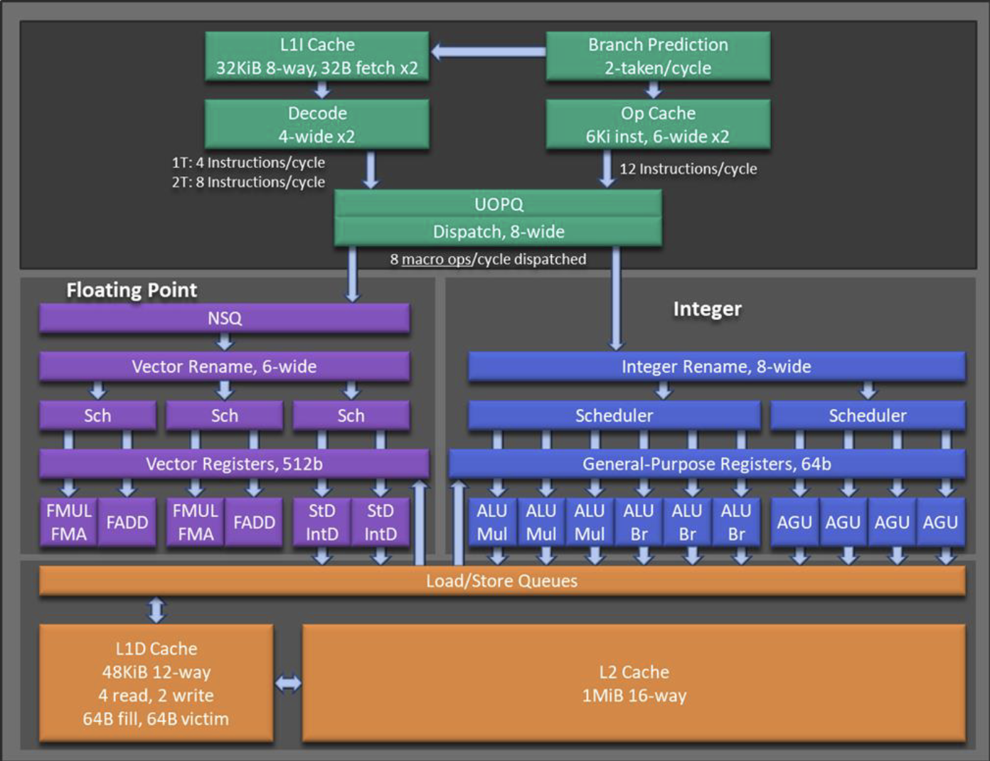
The early kernels were bottlenecked by doing too much work in the integer half: the per-block bswaps ran on the 6 ALUs, and the movd/pinsrd repack queued on the narrow crossing (see image below) between the integer register file and the vector one. That’s the traffic that was quietly outrunning the AES units in variants 2 and 3.
Variant 4 moved the AES kernel computation completely into the SIMD execution units, depicted below.
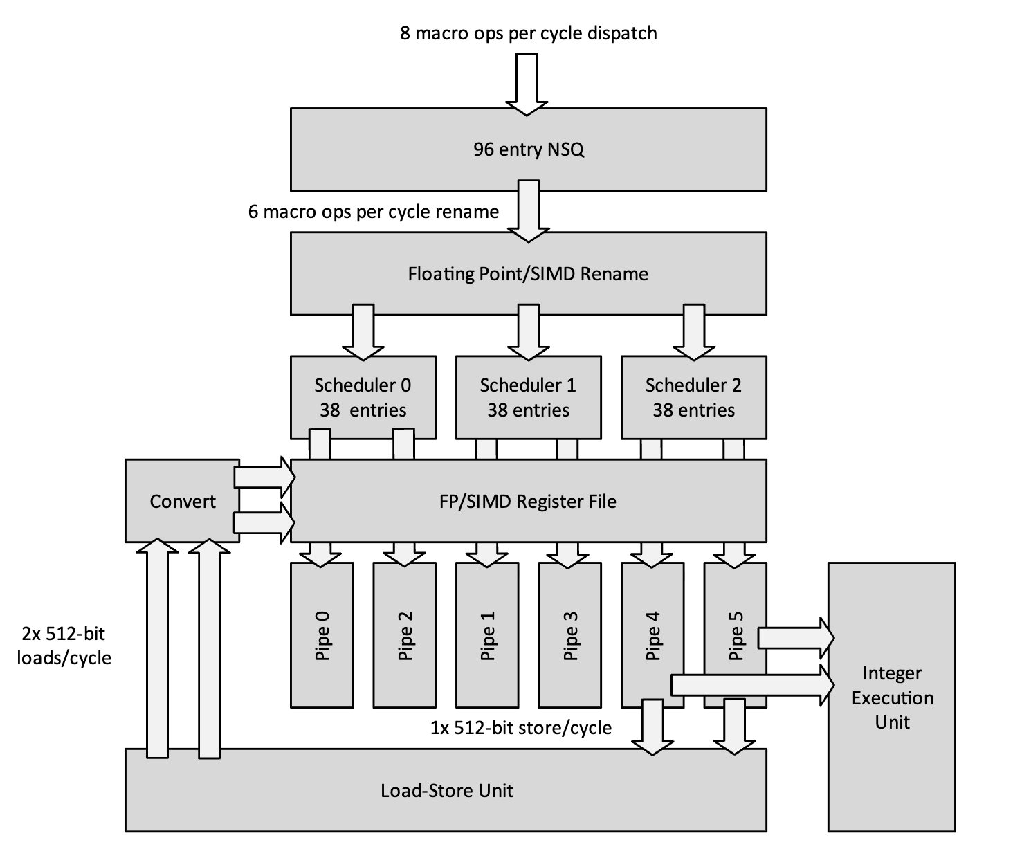
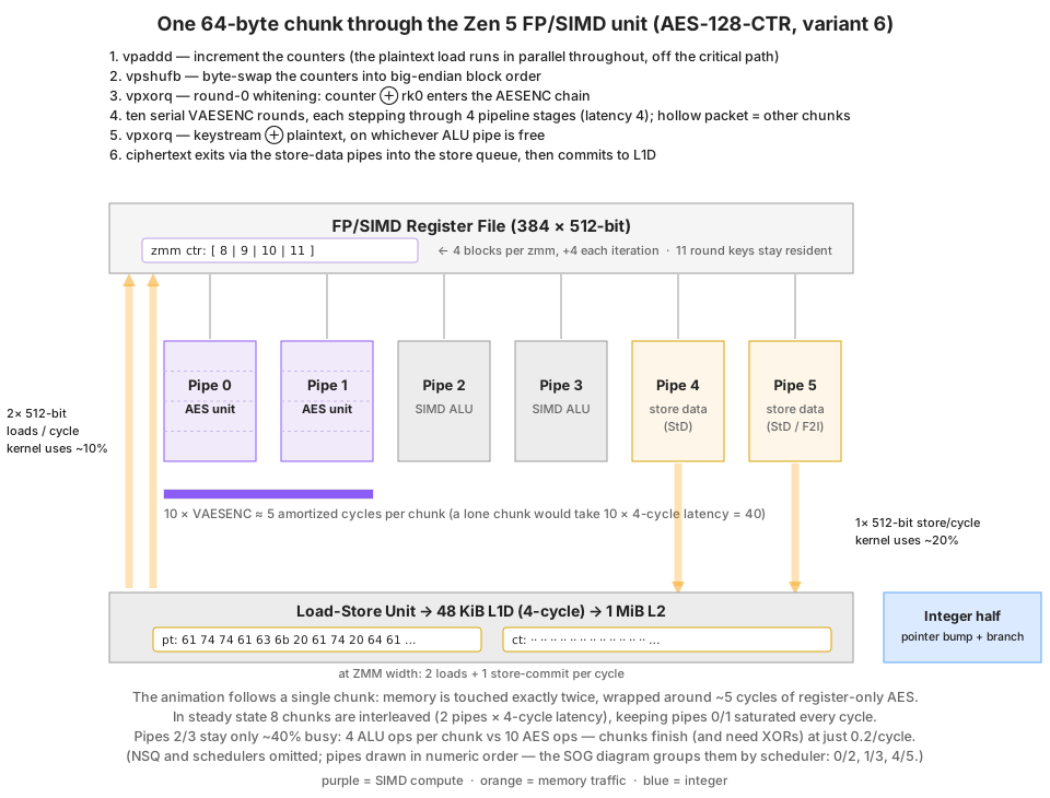
Six SIMD pipes behind three 38-entry schedulers and a 96-entry non-scheduling queue; per uops.info, VAESENC issues on pipes 0 and 1 only — those two pipes at one op/cycle each are the “two AES units” behind every ceiling in this post, and that deep scheduler window is what actually keeps variant 3’s eight independent chains in flight. The left edge is the entire memory interface: 2×512-bit loads and 1×512-bit store per cycle between the vector registers and the load-store unit. In steady state the kernel uses about 10% of the load slots, 20% of the store slots, and ~40% of the two SIMD ALU pipes (only 4 non-AES ops per chunk: counter add, byte-swap, whitening XOR, final XOR — scheduled onto whichever pipe is free, since pipes aren’t wired to each other but all read and write the shared register file) while pipes 0/1 run flat out — the picture of a compute-bound loop. The roofline below asks how far up the cache/DRAM hierarchy that picture survives.
The animation below traces one 64-byte chunk through that picture — counter built in-register, ten rounds ping-ponging between the register file and the two AES pipes while the plaintext load hides underneath, one XOR, one store out:
Roofline: VAES against L1/L2/L3/DRAM
A roofline model asks one question: at your kernel’s arithmetic intensity, which is lower — the compute roof, or the bandwidth line of the memory level your data lives in? Whichever is lower is your ceiling.
For a stream cipher like AES-CTR the arithmetic intensity is trivial and fixed at ½: one byte encrypted per 2 bytes of traffic (one in, one out). Every byte is read once, XORed once, written once.
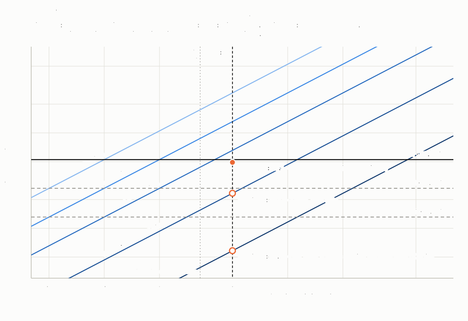
Or in table form, in cycles/byte 11, with per-core numbers from the SOG and from Chips and Cheese’s desktop Zen 5 and Turin measurements:
| where the data lives | per-core bandwidth | feed cost (2 B traffic/B) | vs 0.0841 cyc/B compute roof | verdict |
|---|---|---|---|---|
| L1D | 2×64 B loads + 1×64 B store/cyc | 0.016 cyc/B | 5.4× headroom | compute-bound |
| L2 | 64 B/cyc | 0.031 cyc/B | 2.7× headroom | compute-bound |
| L3 | 32 B/cyc | 0.063 cyc/B | 1.3× headroom | compute-bound — barely |
| DRAM, 1 core | ~50 GB/s ≈ 11 B/cyc | ~0.18 cyc/B | 0.5× | memory-bound |
| DRAM, 8 cores | ~100 GB/s shared ≈ 2.8 B/cyc ea | ~0.70 cyc/B | 0.12× | memory-bound, hard |
Two things fall out of this table.
One core streaming cold data is already memory-bound. A single Zen 5 core can pull roughly 50 GB/s from DRAM — about 11 bytes/cycle at this clock — capping the cipher near 0.18 cyc/B, or ~23 GiB/s: under half the cache-fed 49. And that’s the generous accounting. A plain store to a cold line first reads that line in (write-allocate), making the real traffic 3 B per encrypted byte and the cap more like 15 GiB/s — a third — unless the kernel switches to non-temporal stores. Note what the row does not say: it doesn’t matter whether the cold data arrives as one 20 MiB payload or twenty 1 MiB ones. Fresh bytes cross the DRAM boundary exactly once either way; payload size only decides residency when a benchmark loops over the same buffer, or a real pipeline produces and consumes the data on-chip. That second escape hatch is less exotic than it sounds — the cache-resident assumption isn’t necessarily a benchmarking lie. A TLS server encrypts plaintext its application wrote moments ago, so the data is still cache-hot; on the receive side, server NICs can even DMA packets straight into L3 (Intel calls this DDIO; AMD’s recent EPYCs have Smart Data Cache Injection), so promptly-decrypted traffic may never touch DRAM at all. A well-pipelined server really does feed its cipher from cache — it’s the cold-bulk jobs (encrypting a file at rest, a backlogged queue) that live on the DRAM row.
Eight cores don’t get eight pipes. The compute roofs are per-core and scale with core count; the DRAM line does not. On Turin, a CCD’s eight cores share one GMI link to the IO die, measured at ~100 GB/s of read bandwidth — the socket’s ~500 GB/s of DDR5 is only reachable by spreading across CCDs, which an 8-core VM slice cannot do. So eight cores at full tilt demand ~840 GB/s of traffic from a ~100 GB/s pipe: all eight cores streaming from DRAM deliver roughly what one core delivers from L3. That collapse — 8× the compute against 1× the pipe — is the entire subject of the next post, along with actually measuring these last two rows on this Azure box instead of quoting spec sheets for them.
Footnotes
-
Christof Paar’s AES lecture is a great place to start for those unfamiliar with AES. ↩
-
Meaning we only encrypt, and do not focus on integrity like modern authenticated encryption modes such as AES-GCM. Hence our achieved throughput will naturally be higher than you will find in AEAD benchmarks. ↩
-
If you’ve been DNN-pilled like me, you can see an analogy between the AES network and a deep neural network, with linearities followed by non-linearities. Comparing sigmoids and ReLu to S-boxes is a fun exercise. ↩
-
In fact, block ciphers encrypt blocks (typically 128 bits), whereas stream ciphers encrypt byte streams. The typical AES interface thus takes a bytestream payload, whereas for consistency of our benchmarks we kept the input to all versions as a payload already broken up into
[u32;4]blocks. This is an ugly API but it doesn’t change anything for the purpose of benchmarking. ↩ -
There is an alternative family of designs called ARX (Add-Rotate-XOR) that are constant-time by construction and fast on CPUs. These were pioneered in the late 1980s and 1990s by FEAL, MD4/MD5, and RC5/TEA, and made extremely popular by Daniel Bernstein with his Salsa20 and ChaCha ciphers. When the dedicated AES silicon is present, AES wins in raw throughput: AES-NI is a purpose-built functional unit that does in one instruction what ChaCha does in many ALU ops dispatched through general SIMD ports. Vectorized ChaCha20 runs at ~0.8 cyc/byte with AVX-512, well behind the ~0.1 cyc/byte that VAES reaches with AVX-512. Indeed, a 2025 benchmark shows AES-GCM beating ChaCha20-Poly1305 on all of 9 benchmarked CPUs. ChaCha only wins when AES hardware is absent entirely: ARMv7 phones or ARM SoCs that skip the optional crypto extension, like the Raspberry Pi 3/4’s. ↩
-
AESENC/AESENCLAST on Zen5 have a throughput of 0.5 cycles (two AES units, each accepting one instruction per cycle). AES-128 requires 10 rounds to encrypt a 128 bit (16 bytes) block, thus
10 * 0.5 cycles / 16 bytes = 0.3125 cyc/byte. For more details, see the Appendix section. ↩ ↩2 -
ARMv8’s Cryptographic Extension factors the round differently. x86’s
AESENCis the whole round with the key XORed last:MixColumns(ShiftRows(SubBytes(state))) ⊕ key. ARM splits it in two and XORs the key first:AESEcomputesSubBytes(ShiftRows(state ⊕ key)), andAESMCcomputesMixColumns(state)— so a round is the back-to-back pair, and the final round (which drops MixColumns) is a bareAESEplus one explicit XOR, since there’s noAESENCLASTanalogue. The split exists so that tiny in-order cores can implement each half cheaply; big cores (including Apple’s) recognize the adjacentAESE+AESMCpair at decode and execute it as a single fused µop on the AES unit — same cost as oneAESENC. This is why the two-instruction encoding costs nothing in practice. It’s all on 128-bit NEON registers though, so ARM cores cannot currently compete with x86’s VAES variants 5 and 6, which do two or four blocks per instruction. ↩ -
Intrinsics are compiler built-ins that look like C functions but compile down to one specific machine instruction (the compiler handles register allocation and instruction ordering). Their name encodes their meaning: in
_mm_aesenc_si128, the_mm_prefix (relic of 1996’s MMX, “MultiMedia eXtensions”) marks an x86 SIMD intrinsic and carries the register width (_mm_= 128-bit XMM,_mm256_= YMM,_mm512_= ZMM); the_si128suffix is the operand type —s= scalar,i128= signed 128-bit integer: the register is treated as one undifferentiated 128-bit blob, as opposed to wide VAES intrinsics like_mm256_aesenc_epi128whereepmeans “extended packed”, indicating that twoi128are packed into a 256-bit register. ↩ -
As mentioned in an earlier footnote, the canonical API is to have no block representation at all: blocks stay opaque bytes end to end, and the only byte-order work in all of AES-CTR is a single
PSHUFBon the counter, needed because NIST made the counter field big-endian while_mm_add_epi32counts little-endian — the keystream then XORs straight into the plaintext, no second shuffle. Written that way from the start, variant 3 would have landed near 12 GiB/s on the first try and this entire lesson would have stayed invisible. The wrong representation turned out to be painful but very instructive. ↩ -
Because the CPU and DRAM live in different clock domains, any choice of units is a slight lie. The diagram is in GiB/s with the clock pinned at ~4.4 GHz, which assumes no CPU throttling (lie). The table on the other hand uses cycles instead, to get exact throughput numbers for the caches which sit on the same die as the CPU. The DRAM throughput in seconds is thus a small lie, again assuming the fixed 4.4 GHz conversion. ↩